Chip full-process quality control: Ensuring full-chain protection from source to terminal
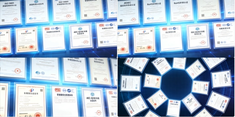
The full-process quality control of chips runs through every key stage from design, manufacturing, packaging and testing to delivery, with the core principle of "prevention first, real-time monitoring, precise traceability, and continuous optimization". A full-life-cycle quality protection system is constructed to ensure the reliability and stability of each chip.
1. Design stage: Quality pre-positioning, risk avoidance from the source
The design stage is the starting point of quality control. Through standardized processes and precise simulations, potential defects are eliminated in advance.
The DFM (Design for Manufacturing) concept is implemented, connecting the requirements of mass production processes at the initial stage of chip architecture design. Through EDA tools, design rule checks (DRC) and layout and schematic consistency checks (LVS) are completed, with defect detection rates exceeding 98%.
Multi-dimensional simulation verification is carried out, covering core indicators such as timing, power consumption, signal integrity (SI), and electromagnetic compatibility (EMC). Reliability simulations under extreme environments are conducted for automotive-grade and industrial-grade chips to ensure that the design meets application requirements.
An IP core quality certification system is established. All reused IPs undergo rigorous stress tests and compatibility verifications, with failure rates controlled below 0.001%, ensuring design quality at the core component level.
2. Wafer manufacturing stage: Real-time monitoring, precise control
Wafer manufacturing is the core环节 of chip production, ensuring process stability through high-precision detection and closed-loop management.
The entire process adopts a Class 100 clean room environment, with real-time monitoring of temperature, humidity, and dust particle counts to avoid quality risks caused by environmental factors.
Online inspection points are set up for key processes, using optical inspection equipment (AOI) and electron beam inspection equipment (EBI) to scan the surface defects of the wafers 100%. The defect density is controlled within 0.1 defects/cm²; 5% of wafers are randomly selected for electrical tests (CP) covering 200+ parameters, with the rejection rate of abnormal batches reaching 100%.
An advanced process control (APC) system is equipped, collecting 1000+ process parameters such as lithography energy, etching pressure, and film thickness. Through AI algorithms, deviations are automatically adjusted, with the fluctuation range of key parameters controlled within ±0.5%, and the process capability index CPK remaining above 1.33.
3. Packaging and testing stage: Multiple verifications, building the factory exit defense line
Packaging and testing are the final quality checkpoint before the chip leaves the factory. Unqualified products are screened through multi-dimensional testing.
The entire packaging process is monitored in real time, using X-Ray to detect solder ball quality and ultrasonic testing to check bonding strength. The void rate of solder balls is below 1%, and the compliance rate of bonding strength is 100%. At the same time, packaging parasitic parameters are strictly controlled to ensure the performance of the chip.
Comprehensive test verification is carried out, including temperature tests at normal, high, and low temperatures, aging tests (HTOL), electrostatic discharge tests (ESD), latch-up tests, etc. For automotive-grade chips, additional rigorous tests such as temperature cycling (-55°C to 125°C) and humidity cycling are conducted to ensure stable operation of the chip in extreme scenarios. The final test (FT) stage adopts parallel testing technology, covering 99.5% of functional and performance indicators, with a final test pass rate of over 99%, and non-compliant products are directly eliminated to prevent defective products from flowing out.
4. Delivery and traceability: Full-process traceability, ensuring the quality loop
The delivery stage continues the quality control efforts, while establishing a full-life-cycle traceability system to achieve rapid problem location and resolution.
The chips are packed with professional anti-static and moisture-proof packaging. During transportation, real-time monitoring of temperature, humidity and vibration conditions is carried out to ensure that the chips are not damaged during delivery. Domestic orders are delivered within 72 hours, and international orders are delivered within 10 days.
Each wafer and each chip is assigned a unique identification code (UID), which records the details of the entire process, including raw material batches, process parameters, test data, and delivery information. The traceability accuracy reaches the level of individual chips. The traceability analysis of any product can be completed within 2 hours.
An after-sales quality feedback mechanism has been established. Quality issues reported by customers are responded to within 24 hours, and solutions are provided within 48 hours. At the same time, problem cases are included in the defect database to provide feedback for process optimization in the front-end design and manufacturing stages.
The entire process of quality control aims for "zero defects". Through seamless connection of each link and strict standards, every chip meets industry norms and customer requirements, providing reliable quality assurance for key fields such as automotive electronics, artificial intelligence, and industrial control.