
Chip process drawings usually include logic circuit diagrams from the design stage, physical circuit diagrams, and mask layout for the manufacturing stage. Here is an introduction to the relevant content:
Logic circuit diagram: It is a circuit diagram obtained by converting the chip function described using hardware description languages (such as Verilog, VHDL, etc.) into a diagram through electronic design automation (EDA) tools. It is used to represent the logic gates, flip-flops, and other components inside the chip and their connection relationships.
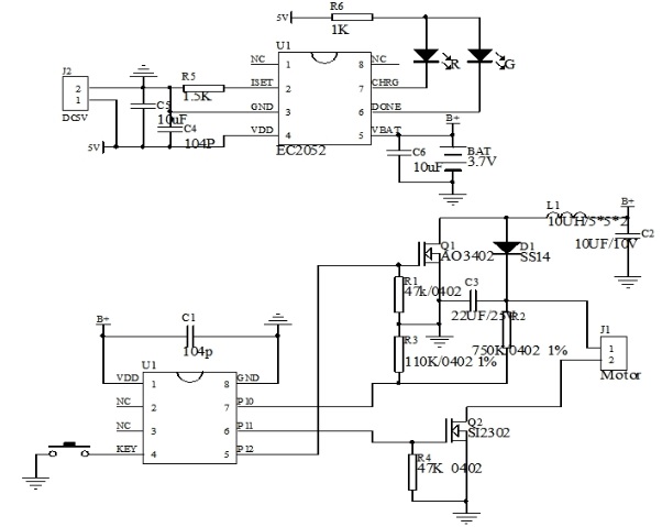
Chip logic circuit diagram
Physical circuit diagram: It is a circuit diagram formed based on logic synthesis, after circuit layout and routing (Place And Route). It takes into account factors such as the physical layout and wiring rules of the chip, converting the logic circuit into an actual physical structure. Different colors in the diagram usually represent different mask layers.
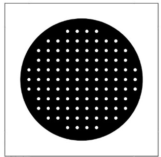
Chip physical circuit diagram
Photolithography mask layout: It is a drawing used in the photolithography process, which transfers the circuit patterns of the chip onto the wafer. The patterns on the photolithography mask layout correspond to the final circuit structure of the chip. Through the exposure operation of the photolithography machine, the patterns on the mask are replicated onto the surface of the wafer coated with photolithography resin.
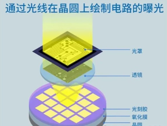
Chip lithography mask layout
Process flow diagram: Presenting the entire manufacturing process of the chip in a graphical format, including the main steps such as wafer manufacturing, lithography, etching, ion implantation, and film deposition, along with their sequence of occurrence.